


| Place of Origin: | Guangdong, China |
|---|---|
| Brand Name: | CANYI |
| Certification: | RoHS |
| Model Number: | 3N80 |
| Minimum Order Quantity: | Negotiable |
| Price: | Negotiated |
| Packaging Details: | Dimensions per Unit:19*6.3*21 centimeter • Weight per Unit:100g• Units per Export Carton:10000 • Export Carton Dimensions L/W/H: 42*33*24 centimeter• Export Carton Weight:3 Kilograms |
| Delivery Time: | 3-5 days |
| Payment Terms: | Telegraphic Transfer in Advance (Advance TT, T/T) |
| Supply Ability: | 15,000,000PCS Per Day |
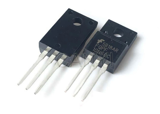
| Type: | N-Channel Power MOSFET | Package: | ITO-220 |
|---|---|---|---|
| Drain-Source Voltage: | 800v | Continuous Drain Current: | 3A |
| Package Type: | Throught Hole | Samples: | Free |
| High Light: | mosfet power transistor,high power transistor |
||
800V n channel transistor 3N80 mosfet ITO220 field effect transistor
20~40V 40V 55-60V 65-95V 100-150V 200-500V 600V 650V 700-900V MOSFET
High power transistor features:
The 3N80 provide excellent RDS(ON)low gate charge and operation with low gate voltages. This device is suitable for use as a load switch or in PWM applications.It used in power switching application.
| Parameter | Symbol | Limit | Unit |
| Drain-Source Voltage | VDS | 800 | V |
| Gate-Source Voltage | VGS | ±30 | |
| Continuous Drain Current | ID | 3 | A |
|
Pulsed Drain Current |
IDM | 10 | |
| Single Pulsed Avalanche Energy (note1) |
EAS
|
170 |
mJ
|
| Thermal Resistance from Junction to Ambient |
RθJA
|
62.5 |
℃/W
|
| Junction Temperature | TJ | 150 |
℃
|
| Storage Temperature Range | TSTG | -55~+150 | |
|
Maximum lead temperature for soldering purposes , 1/8”from case for 5 seconds |
TL
|
260 |
| Parameter | Symbol | Test Condition | Min. | Typ. | Max. | Unit |
| Off Characteristics | ||||||
| Drain-Source Breakdown Voltage | V(BR) DSS | VGS = 0V, ID = -250uA | 800 | V | ||
| Zero Gate Voltage Drain Current | IDSS | VDS = 800V, VGS = 0V | 1 | uA | ||
| Gate Body Leakage | IGSS | VGS=±30v,VDS= 0V | ±100 | nA | ||
| On characteristics (note 2) | ||||||
| Drain-Source On-State Resistance | RDS(on) | VGS = 10V, ID = 1.5A | 4.2 | mΩ | ||
| Forward Transconductance 1) | gfs | VDS=1 5V,ID= 1.5A | 2.1 | S | ||
| Gate Threshold Voltage | VGS(th) | VDS = VGS ,ID = 250uA | 3 | 4.5 | v | |
| Switching Characteristics (note 2,3) | ||||||
| Turn-On Delay Time | td(on) |
VDD = 400V, VDS=10V RG=4.7Ω,RG = 3A |
17 | ns | ||
| Turn-On Rise Time | tr | 27 | ||||
| Turn-Off Delay Time | td(off) | 36 | ||||
| Turn-Off Fall Time | tf | 40 | ||||
| Total Gate Charge | Qg |
VDS =640V,VGS =10V,ID =3A
|
19 | nC | ||
| Gate-Source Charge | Qgs | 32 | nC | |||
| Gate-Drain Charge | Qgd | 10.8 | nC | |||
| Dynamic Characteristics (note 3) | ||||||
| Input Capacitance | Ciss |
VDS = 25V, VGS = 0V f = 1 MHz
|
485 | pF | ||
| Output Capacitance | Coss | 57 | ||||
| Reverse Transfer Capacitance | Crss | 11 | ||||
| Drain-source diode characteristics and maximum ratings | ||||||
| Drain-source diode forward voltage | VSD | VGS = 0V, IS =3A | 1.6 | V | ||
|
Continuous drain-source diode forward current
|
IS
|
3 | A | |||
|
Pulsed drain-source diode forward current
|
ISM
|
10 | A | |||
Choose Canyi to get more benefit:
Our fast delivery time can be in just one to two weeks for urgent demands. Providing customers with flexible, safe and efficient logistics services.For a electronic information base component supplier, contact us today.
![]()
Contact:Wendy Yan
Email:wendy@zd_schottkysignal.com
Whatsapp/Wechat:+86 13423609933
Skype:wendy@doublelight.com.cn

