


| Place of Origin: | Guangdong, China |
|---|---|
| Brand Name: | NCE |
| Certification: | RoHS |
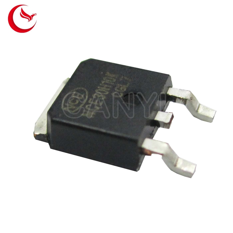
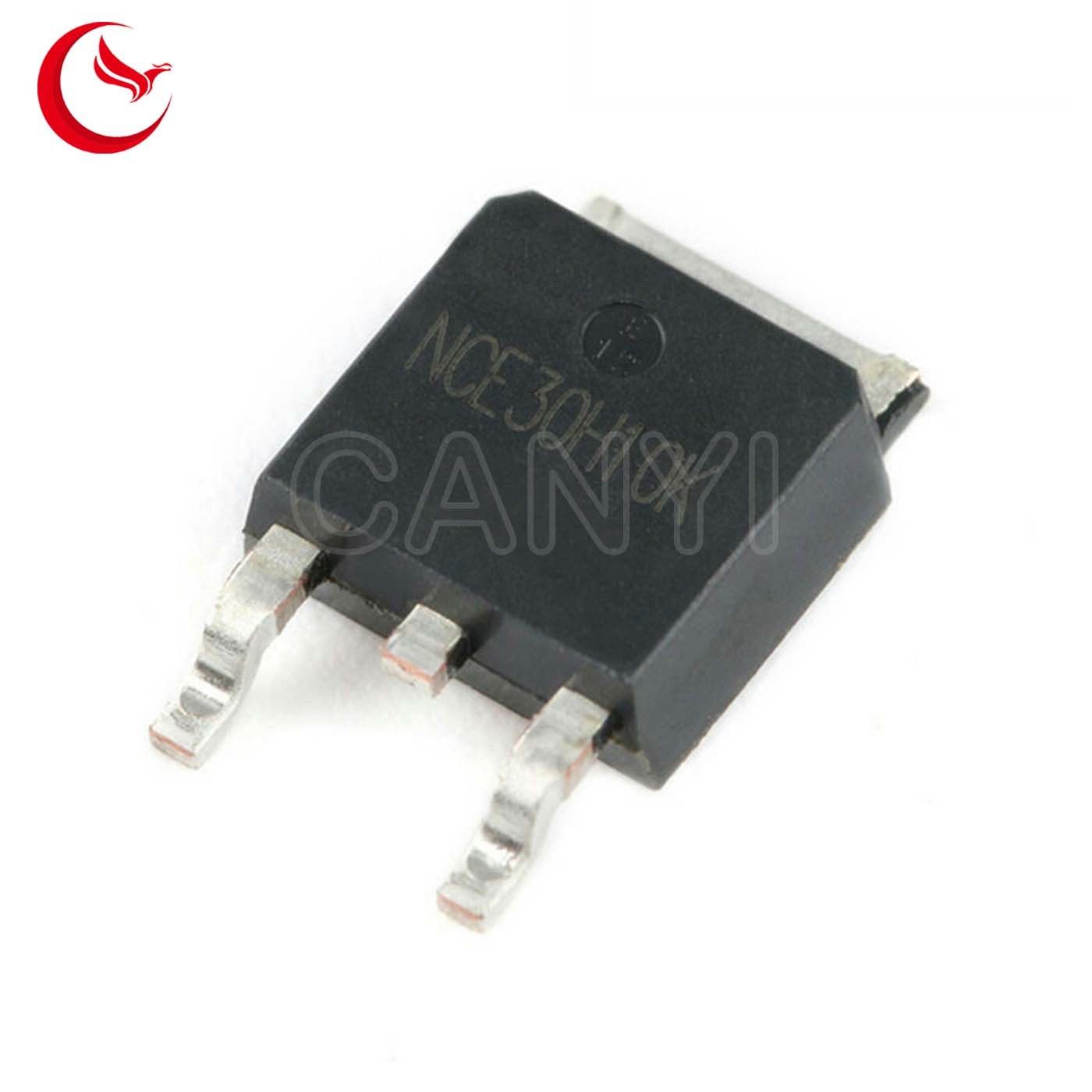
| Model Number: | NCE30H10K |
| Minimum Order Quantity: | 2500PCS |
| Price: | usd 0.2/pcs |
| Packaging Details: | Dimensions per Unit:19*6.3*21 centimeter • Weight per Unit:100g• Units per Export Carton:10000 • Export Carton Dimensions L/W/H: 42*33*24 centimeter• Export Carton Weight:3 Kilograms |
| Delivery Time: | 3-5 days |
| Payment Terms: | Telegraphic Transfer in Advance (Advance TT, T/T) |
| Supply Ability: | 15,000,000PCS Per Day |
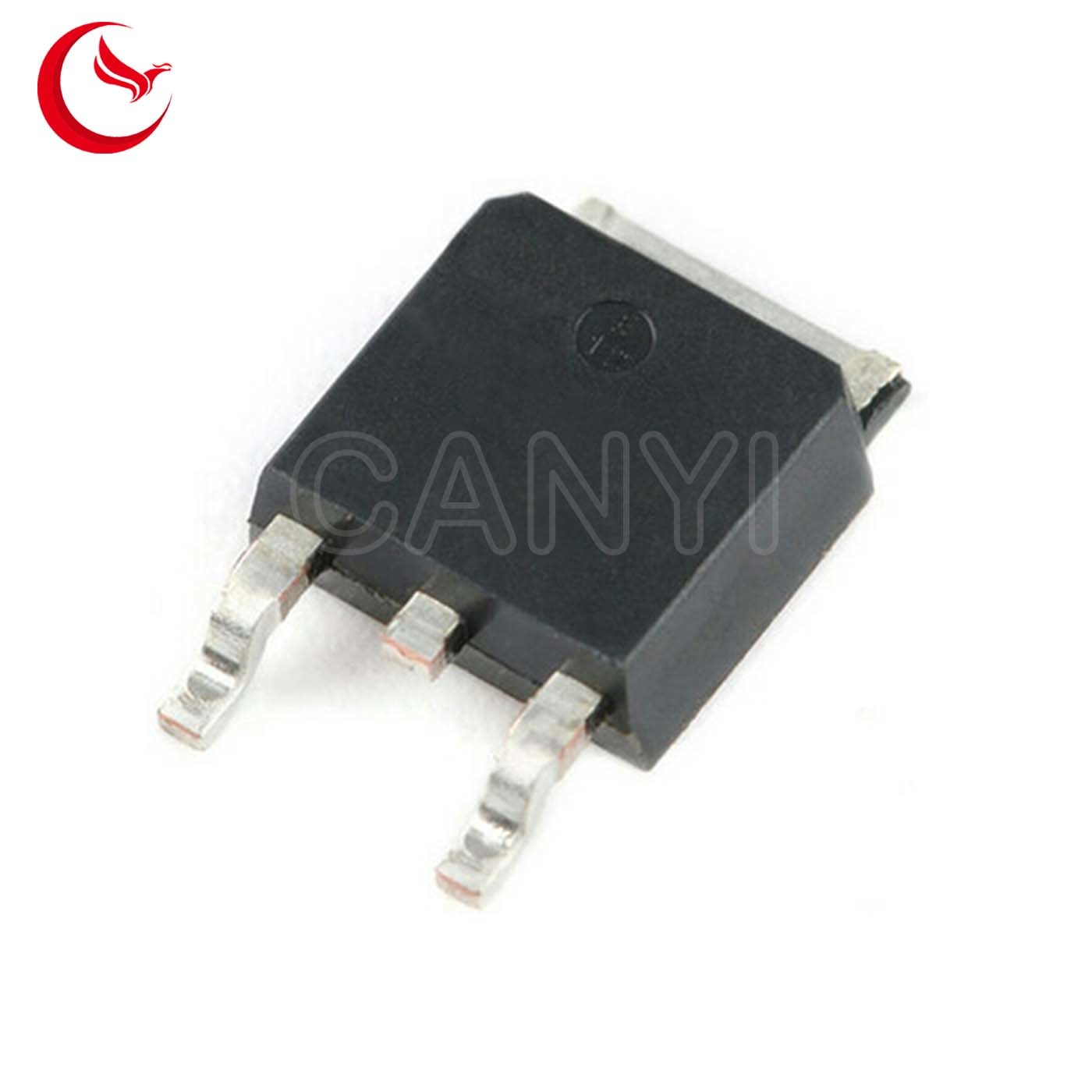
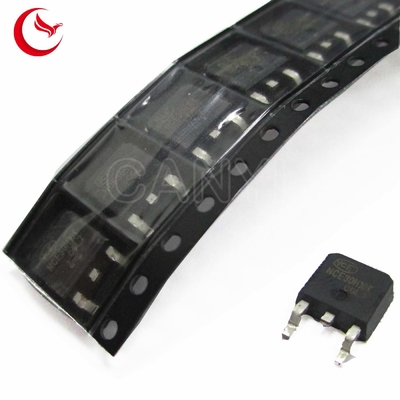
| Type: | NCE N Channel MOSFET | Package Type: | Surface Mount |
|---|---|---|---|
| Package: | TO-252 | VDS: | 30V |
| Drain Current-Continuous: | 100A | Maximum Power Dissipation: | 110W |
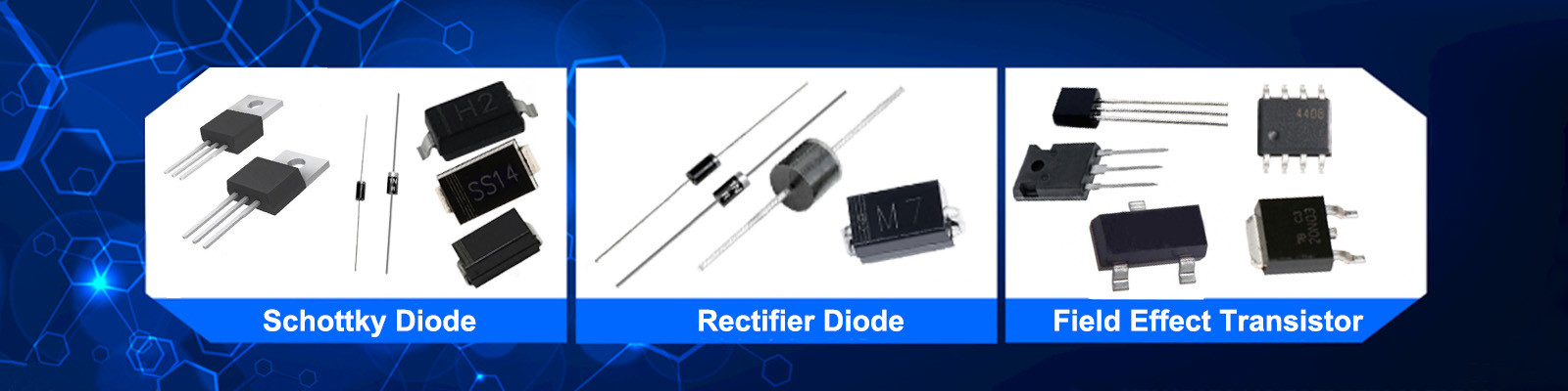
| High Light: | NCE N Channel MOSFET,NCE30H10K Surface Mount MOSFET,TO-252 Surface Mount MOSFET |
||
AO3400 SOT-23 mosfet power transistor NPN MOSFET A09T n channel transistor
N channel transistor features
| Parameter | Symbol | Limit | Unit |
| Drain-Source Voltage | VDS | 800 | V |
| Gate-Source Voltage | VGS | ±30 | |
| Continuous Drain Current | ID | 100 | A |
| IDM | 400 | |
Maximum Power Dissipation | PD | 110 | W |
Single pulse avalanche energy ( | EAS | 350 | mJ |
Operating Junction and Storage Temperature Range | TJ,TSTG | -55 To 175 | ℃ |
Electrical Characteristics (TA=25°C, unless otherwise noted)
| Parameter | Symbol | Test Condition | Min. | Typ. | Max. | Unit |
| Off Characteristics | ||||||
| Drain-Source Breakdown Voltage | V(BR) DSS | VGS = 0V, ID = -250uA | 30 | - | - | V |
| Zero Gate Voltage Drain Current | IDSS | VDS = 24V, VGS = -0V | - | - | 1 | uA |
| Gate Body Leakage | IGSS | VGS=±12v,VDS= 0V | - | - | ±100 | nA |
| On characteristics | ||||||
| Gate Threshold Voltage | VGS(th) | VDS = VGS ,ID = 250uA | 1 | 1.6 | 3 | v |
| Drain-Source On-State Resistance | RDS(ON) | VGS=10V, ID=20A | - | 4.0 | 5.5 | mΩ |
| Forward Transconductance | gfs | VDS= 10V,ID= 20A | 50 | - | - | S |
| Switching Characteristics | ||||||
| Turn-On Delay Time | td(on) | VDD = 15V, ID=60A | - | 11 | - | ns |
| Turn-On Rise Time | tr | - | 160 | - | ||
| Turn-Off Delay Time | td(off) | - | 25 | - | ||
| Turn-Off Fall Time | tf | - | 60 | - | ||
Total Gate Charge | Qg | VDS=15V,ID=30A, | 70 | nC | ||
Gate-Source Charge | Qgs | 8.8 | ||||
Gate-Drain Charge | Qgd | 16.3 | ||||
| Dynamic Characteristics | ||||||
| Input Capacitance | Ciss | | 3400 | pF | ||
| Output Capacitance | Coss | 356 | ||||
| Reverse Transfer Capacitance | Crss | 308 | ||||
| Drain-source diode characteristics | ||||||
| Diode Forward Voltage | VSD | ISD=20A,VGS=0V | - | - | 1.2 | V |
| Diode Forward Current | IS | - | - | - | 100 | A |
| Reverse Recovery Time | trr | Tj=25℃,Isd=60A, | - | 56 | - | ns |
| Reverse Recovery Charge | Qrr | - | 110 | - | nC | |