
| Place of Origin: | Guangdong, China |
|---|---|
| Brand Name: | CANYI |
| Certification: | RoHS |
| Model Number: | TW60N06C |
| Minimum Order Quantity: | Negotiable |
| Price: | Negotiated |
| Packaging Details: | Dimensions per Unit:19*6.3*21 centimeter • Weight per Unit:100g• Units per Export Carton:10000 • Export Carton Dimensions L/W/H: 42*33*24 centimeter• Export Carton Weight:3 Kilograms |
| Delivery Time: | 3-5 days |
| Payment Terms: | Telegraphic Transfer in Advance (Advance TT, T/T) |
| Supply Ability: | 15,000,000PCS Per Day |
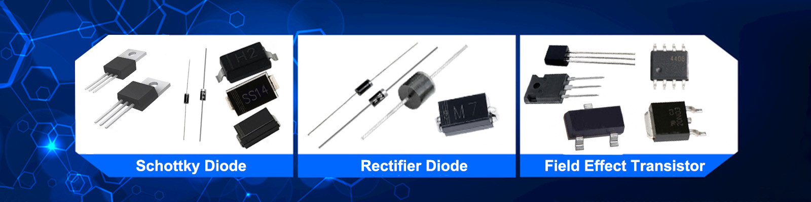
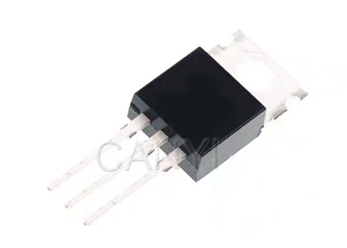
| Type: | N Channel MOSFET Transistor | Package Type: | THT |
|---|---|---|---|
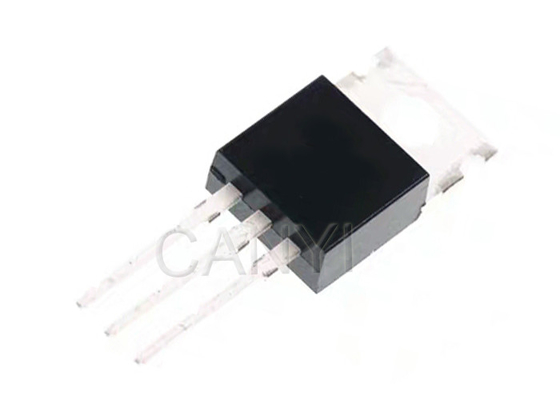
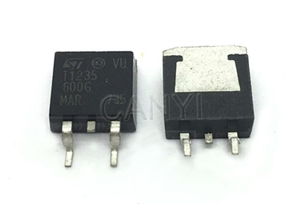
| Package: | TO-220 TO-263 | VDS: | 60V |
| Maximum Power Dissipation: | 115W | Sample: | Free |
| Highlight: | mosfet power transistor,high power transistor |
||
60V TO-263 n channel transistor TO-220 advanced power field effect transistor
Mosfet n channel features:
Maximum Ratings and Thermal Characteristics (TA = 25℃unless otherwise note
| Parameter | Symbol | Limit | Unit |
| Drain-Source Voltage | VDS | 60 | V |
| Gate-Source Voltage | VGS | ±20 | |
| Continuous Drain Current | ID | 60 | A |
|
|
IDM | 45 | |
| Power Dissipation | PD | 115 | W |
| Junction Temperature | TJ | -55~+175 | ℃ |
| Storage Temperature | TSTG | -55~+175 | ℃ |
Electrical Characteristics (TA=25°C, unless otherwise noted)
| Parameter | Symbol | Test Condition | Min. | Typ. | Max. | Unit |
| Static Electrical Characteristics @ TC = 25°C (unless otherwise stated) | ||||||
| Drain-Source Breakdown Voltage | V(BR) DSS | VGS = 0V, ID = -250uA | 60 | - | - | V |
| Zero Gate Voltage Drain Current(Tc=25℃) |
IDSS
|
VDS = 60V, VGS = 0V | - | - | 1 | uA |
| Zero Gate Voltage Drain Current(Tc=125℃) | VDS = 60V, VGS = 0V | - | - | 100 | ||
| Gate-Body Leakage Current | IGSS | VGS=±20v,VDS= 0V | - | - | ±100 | nA |
| Drain-Source On-State Resistance(Note 3) | RDS(on) | VGS=10V, ID=40A | - | 9 | 12 | mΩ |
| Dynamic Electrical Characteristics @ T C= 25°C (unless otherwise stated) | ||||||
| Input Capacitance | Ciss |
VDS = 24V, VGS = 0V f = 1 MHz |
- | 1860 | - | pF |
| Output Capacitance | Coss | - | 150 | - | ||
| Reverse Transfer Capacitance | Crss | - | 95 | - | ||
| Total Gate Charge | Qg |
VDS=30V,ID=10A, VGS=10V |
- | 26 | - | nC |
| Gate-Source Charge | Qgs | - | 6.5 | - | ||
| Gate-Drain Charge | Qgd | - | 4.5 | - | ||
| Switching Characteristics | ||||||
| Turn-On Delay Time | td(on) |
VDD = 30V,,ID=10A, RG = 6.8Ω,VDS=10V
|
- | 9 | - | ns |
| Turn-On Rise Time | tr | - | 5 | - | ||
| Turn-Off Delay Time | td(off) | - | 28 | - | ||
| Turn-Off Fall Time | tf | - | 4 | - | ||
| Source- Drain Diode Characteristics@ TC = 25°C (unless otherwise stated) | ||||||
| Diode Forward Voltage | VSD | ISD=40A,VGS=0V | - | 0.91 | 1.2 | V |
| Reverse Recovery Time | trr |
Tj=25℃,Isd=20A, VGS=0V di/dt=100A/μs |
- | 23 | - | ns |
| Reverse Recovery Charge | Qrr | - | 52 | - | nC | |
Note :
1.Pulse width ≤ 300μs; duty cycle≤ 2%.
We are professional Electronic Components at competitive price,located in Shenzhen City,China.
Should you have any inquires or comments,we would be glad to talk in details through skype/email/Wechat/WhatsApp or any way you like.
Contact:Wendy Yan
Email:wendy@zd_schottkysignal.com
Whatsapp/Wechat:+86 13423609933
Skype:wendy@doublelight.com.cn

