


| Place of Origin: | shenzhen, China |
|---|---|
| Brand Name: | CANYI |
| Certification: | RoHS |
| Model Number: | AP60N03DF |
| Minimum Order Quantity: | 1000PCS |
| Price: | Negotiated |
| Packaging Details: | Dimensions per Unit:19*6.3*21 centimeter • Weight per Unit:100g• Units per Export Carton:10000 • Export Carton Dimensions L/W/H: 42*33*24 centimeter• Export Carton Weight:3 Kilograms |
| Delivery Time: | 3-7 days |
| Payment Terms: | Telegraphic Transfer in Advance (Advance TT, T/T) |
| Supply Ability: | 15,000,000PCS Per Day |
| Type: | Plastic Transistor | Application: | Battery Protection Or In Other Switching |
|---|---|---|---|
| Reverse Transfer Capacitance: | 131pF | Forward Transconductance: | 9.8S |
| Avalanche Current: | 34A | Storage Temperature Range: | -55 To 150 ℃ |
| High Light: | mosfet power transistor,high power transistor |
||
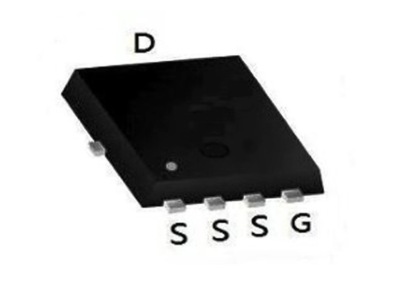
AP60N03DF N-Channel Advanced Power MOSFET power field effect transistor
AP60N03DF.pdf
Description
The AP60N03DF uses advanced trench technology to provide excellent R DS(ON) , low gate charge and operation with gate voltages as low as 4.5V. This device is suitable for use as a Battery protection or in other Switching application.
General Features
V DS = 30V I D =60 A
R DS(ON) < 8.5mΩ @ V GS =10V
Application
Battery protection
Load switch
Uninterruptible power supply
![]()
![]()
Absolute Maximum Ratings (TC=25℃unless otherwise noted)
| Parameter | Symbol | Limit | Unit |
| Drain-Source Voltage | VDS | 30 | V |
| Gate-Source Voltage | VGS | ±20 | V |
| Continuous Drain Current, V GS @ 10V 1 | I D @T C =25 ℃ | 60 | A |
| Continuous Drain Current, V GS @ 10V 1 | I D @T C =100 ℃ | 29 | |
| Continuous Drain Current, V GS @ 10V 1 | I D @T A =25℃ | 11 | A |
| Continuous Drain Current, V GS @ 10V 1 | I D @T A =70℃ | 9 | A |
| Pulsed Drain Current 2 | I DM | 92 | A |
| Single Pulse Avalanche Energy 3 | EAS | 57.8 | mJ |
| Avalanche Current | I AS | 34 | A |
| Total Power Dissipation 4 | P D @T C =25℃ | 29 | W |
| Total Power Dissipation 4 | P D @T A =25 ℃ | 1.67 | W |
| Storage Temperature Range | T STG | -55 to 150 | ℃ |
| Operating Junction Temperature Range | T J | -55 to 150 | ℃ |
| Thermal Resistance Junction-ambient 1 |
R θJA | 75 | ℃ /W |
| Thermal Resistance Junction-Case 1 | R θJC | 4.32 | ℃ /W |
Electrical Characteristics (TJ=25 ℃, unless otherwise noted)
| Parameter | Symbol | Condition | Min | Typ | Max | Unit |
| Drain-Source Breakdown Voltage | BV DSS | V GS =0V I D =250μA | 30 | - | - | V |
| BVDSS Temperature Coefficient | △BV DSS /△T J | Reference to 25℃ ,I D =1mA | - | 0.027 | - | V/℃ |
| Static Drain-Source On-Resistance 2 | R DS(ON) | V GS =10V , I D =12A | - | 7 | 8.5 | mΩ |
| V GS =4.5V , I D =10A | 10 | 1.3 | ||||
| Gate Threshold Voltage | VGS(th) | V GS =V DS , I D =250uA | 1.0 | - | 2.5 | V |
| V GS(th) Temperature Coefficient | △V GS(th | - | -5.8 | - | mV/℃ | |
| Drain-Source Leakage Current | I DSS |
V DS =24V , V GS =0V , T J =25℃ |
- | - | 1 | uA |
|
V DS =24V , V GS =0V , T J =55℃ |
- | - | 5 | |||
| Gate-Source Leakage Current | I GSS | V GS =±20V , V DS =0V | - | - | ± 100 | nA |
| Forward Transconductance | gFS | V DS =5V , I D =15A | - | 9.8 | - | S |
| Gate Resistance | R g | V DS =0V , V GS =0V ,f=1MHz | - | 1.7 | - | |
| Total Gate Charge (4.5V) | Q g |
V DS =20V , V GS =4.5V , I D =12A |
- | 12.8 | - | nC |
| Gate-Source Charge | Q gs | - | 3.3 | - | ||
| Gate-Drain Charge | Q gd | - | 6.5 | - | ||
| Turn-on Delay Time | td(on) |
V DD =12V , V GS =10V , R G =3.3 I D =5A |
- | 4.5 | - | nS |
| Rise Time | t r | - | 10.8 | - | ||
| Turn-Off Delay Time | td(off) | - | 25.5 | - | ||
| Fall Time | t f | - | 9.6 | - | ||
| Input Capacitance | C iss | V DS =15V , V GS =0V ,f=1MHz | - | 1317 | - | pF |
| Output Capacitance | C oss | - | 163 | - | ||
| Reverse Transfer Capacitance | C rss | - | 131 | - | ||
| Continuous Source Current 1,6 | I S | V G =V D =0V , Force Current | - | - | 46 | A |
| Pulsed Source Current 2,6 | I SM | - | - | 92 | A | |
| Diode Forward Voltage 2 | VSD | V GS =0V , I S =1A ,T J =25℃ | - | - | 1 | V |
Diode Characteristics
Note :
1.The data tested by surface mounted on a 1 inch 2 FR-4 board with 2OZ copper.
2.The data tested by pulsed , pulse width ≦ 300us , duty cycle ≦ 2%
3 .The EAS data shows Max. rating . The test condition is V DD =25V,V GS =10V,L=0.1mH,I AS =34A
4.The power dissipation is limited by 150℃ junction temperature
5 .The data is theoretically the same as I D and I DM , in real applications , should be limited by total power dissipation.
![]()

