


| Place of Origin: | shenzhen, China |
|---|---|
| Brand Name: | CANYI |
| Certification: | RoHS |
| Model Number: | AP50P03NF |
| Minimum Order Quantity: | 1000PCS |
| Price: | Negotiated |
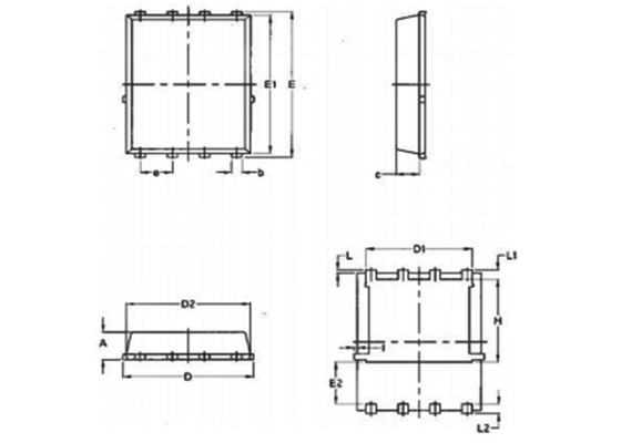
| Packaging Details: | Dimensions per Unit:19*6.3*21 centimeter • Weight per Unit:100g• Units per Export Carton:10000 • Export Carton Dimensions L/W/H: 42*33*24 centimeter• Export Carton Weight:3 Kilograms |
| Delivery Time: | 3-7 days |
| Payment Terms: | Telegraphic Transfer in Advance (Advance TT, T/T) |
| Supply Ability: | 15,000,000PCS Per Day |
| Type: | Plastic Transistor | Application: | Aload Switch Or In PWM |
|---|---|---|---|
| Forward Transconductance: | 20S | Drain-Source Breakdown Voltage: | -33V |
| Single Pulse Avalanche Energy: | 231mJ | Operating Junction And Storage Temperature Range: | -55 To 150 ℃ |
| High Light: | mosfet power transistor,high power transistor |
||
AP50P03NF P-Channel Advanced Power MOSFET field effect high voltage transistor
AP50P03NF.pdf
Description
The AP50P03NF uses advanced trench technology to provide excellent R DS(ON) , low gate charge and operation with gate voltages as low as 4.5V. This device is suitable for use as aload switch or in PWM applications.
General Features
V DS = -30V,I D = -50A
R DS(ON) < 18mΩ @ V GS =-4.5V
R DS(ON) < 13mΩ @ V GS =-10V
High Power and current handing capability
Lead free product is acquired
Surface mount package
Application
PWM applications
Load switch
Power management
![]()
![]()
Absolute Maximum Ratings (TC=25℃unless otherwise noted)
| Parameter | Symbol | Limit | Unit |
| Drain-Source Voltage | VDS | -30 | V |
| Gate-Source Voltage | VGS | ±20 | V |
| Drain Current-Continuous (T C =25℃) | I D | -50 | A |
| Drain Current-Continuous (T C =100℃) | -24 | ||
| Drain Current-Pulsed (Note 1) |
IDM | -80 | A |
| Maximum Power Dissipation (T C =25℃) | P D | 3 | W |
| Maximum Power Dissipation (T C =100℃) | 1.3 | ||
| Single pulse avalanche energy (Note 5) |
EAS | 231 | mJ |
| Operating Junction and Storage Temperature Range | TJ,TSTG | -55 To 150 | ℃ |
| Thermal Resistance,Junction-to-Ambient (Note 2) |
RθJA | 41.67 | ℃ /W |
Electrical Characteristics (TJ=25 ℃, unless otherwise noted)
| Parameter | Symbol | Condition | Min | Typ | Max | Unit |
| Drain-Source Breakdown Voltage | BV DSS | V GS =0V I D =-250μA | -30 | -33 | - | V |
| Zero Gate Voltage Drain Current | IDSS | V DS =-30V,V GS =0V | - | - | -1 | μA |
| Gate-Body Leakage Current | IGSS | V GS =±20V,V DS =0V | - | - | ±100 | nA |
| Gate Threshold Voltage | VGS(th) | V DS =V GS ,I D =-250μA | -1 | -1.5 | -3 | V |
| Drain-Source On-State Resistance | RDS(ON) | V GS =-10V, I D =-10A | - | 11.5 | 15 | mΩ |
| V GS =-4.5V, I D =-7A | - | 18 | 25 | mΩ | ||
| Forward Transconductance | gFS | V DS =-10V,I D =-10A | - | 20 | - | S |
| Input Capacitance | C lss | V DS =-15V,V GS =0V,F=1.0MHz | - | 1750 | - | PF |
| Output Capacitance | Coss | - | 215 | - | PF | |
| Reverse Transfer Capacitance | C rss | - | 180 | - | PF | |
| Turn-on Delay Time | td(on) |
V DD =-15V, ID=-10A,V GS =-10V, R GEN =1Ω |
- | 9 | - | nS |
| Turn-on Rise Time | t r | - | 8 | - | nS | |
| Turn-Off Delay Time | td(off) | - | 28 | - | nS | |
| Turn-Off Fall Time | t f | - | 10 | - | nS | |
| Total Gate Charge | Q g | V DS =-15V,I D =-10A,V GS =-10V | - | 24 | - | nC |
| Gate-Source Charge | Q gs | - | 3.5 | - | nC | |
| Gate-Drain Charge | Q gd | - | 6 | - | nC | |
| Diode Forward Current (Note 2) |
I S | - | - | -12 | A | |
| Diode Forward Voltage (Note 3) |
VSD | V GS =0V,I S =-12A | - | - | -1.2 | V |
Notes:
1. Repetitive Rating: Pulse width limited by maximum junction temperature.
2. Surface Mounted on FR4 Board, t ≤ 10 sec.
3. Pulse Test: Pulse Width ≤ 300μs, Duty Cycle ≤ 2%.
4. Guaranteed by design, not subject to production
5. E AS condition: Tj=25℃,V DD =-15V,V G =10V,L=0.5mH,Rg=25Ω, I AS =-34A
![]()
![]()
![]()
![]()
For more information please refer to the attachment, or contact us:
Contact: Roundy
Tel: 86-755-82853859
Fax: 86-755-83229774
Email:Roundy@doublelight.com.cn
Wechat:15216951191
Skype:Roundy@doublelight.com.cn
Whatsapp:+86 15216951191
![]()

