


| Place of Origin: | Guangdong, China |
|---|---|
| Brand Name: | CANYI |
| Certification: | RoHS |
| Model Number: | AP70N03NF |
| Minimum Order Quantity: | 1000PCS |
| Price: | Negotiated |
| Packaging Details: | Dimensions per Unit:19*6.3*21 centimeter • Weight per Unit:100g• Units per Export Carton:10000 • Export Carton Dimensions L/W/H: 42*33*24 centimeter• Export Carton Weight:3 Kilograms |
| Delivery Time: | 3-5 days |
| Payment Terms: | Telegraphic Transfer in Advance (Advance TT, T/T) |
| Supply Ability: | 15,000,000PCS Per Day |
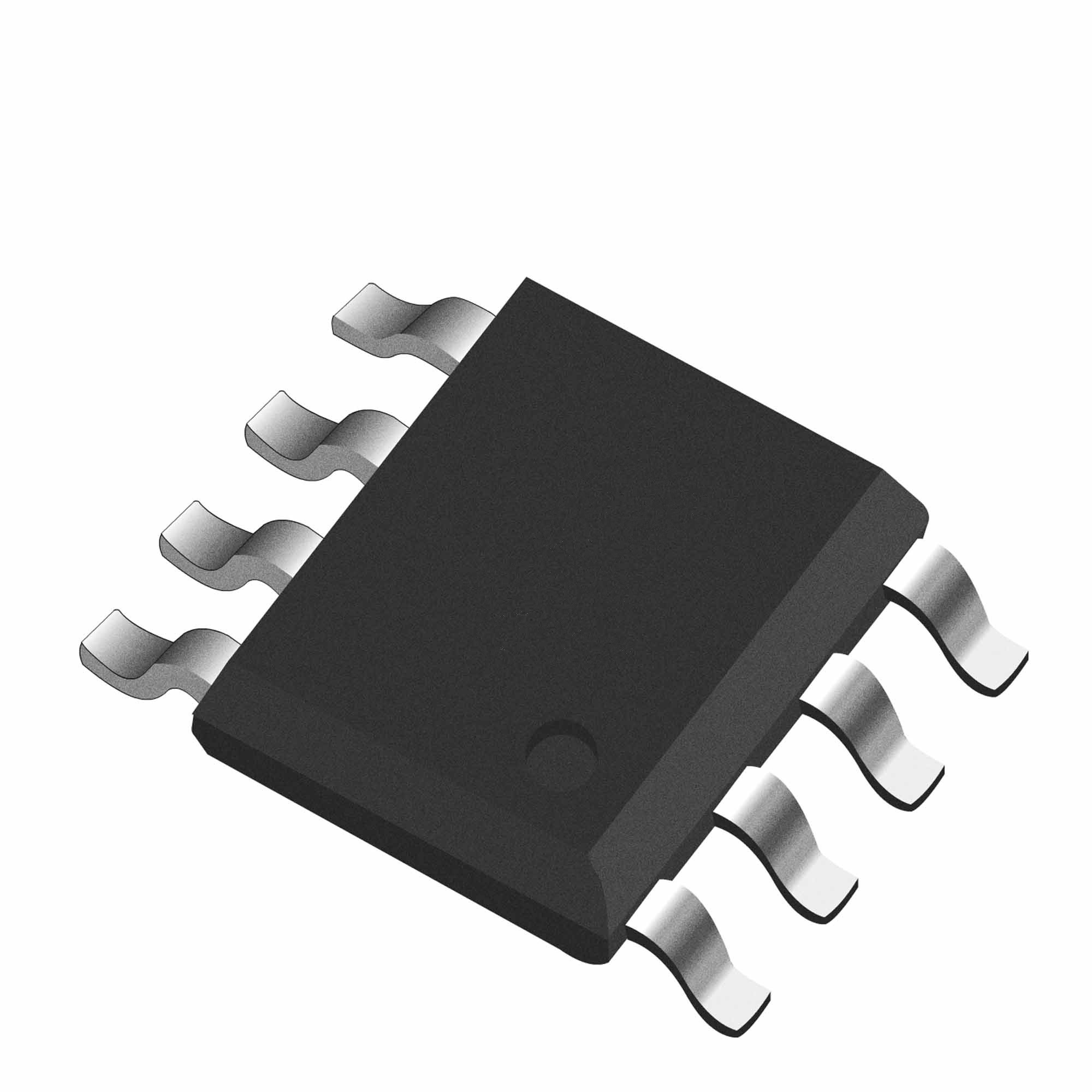
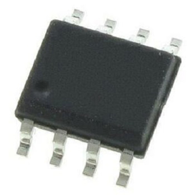
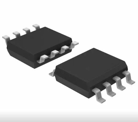
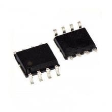
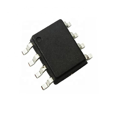
| Type: | Plastic Transistor | Package: | SOP-8 |
|---|---|---|---|
| TJ, Tstg: | -55 To 150℃ | Shipping By: | DHL\UPS\Fedex\EMS\HK Post |
| Lead Time: | 2-3days | Application: | For VCD, DVD, Calculator, Etc. |
| High Light: | mosfet power transistor,high power transistor |
||
AP70N03NF.pdfAP70N03NF Transistor MOSFET SMD N-Channel Electronic Component for Integrated Circuit
Description
The AP70N03NF uses advanced trench technology to provide excellent RDS(ON), low gate 6][charge and operation with gate voltages as low as 4.5V. This device is suitable for use as a
Battery protection or in other Switching application.
General Features
VDS = 30V ID =70A
RDS(ON) < 5.5mΩ VGS=10V
N-Channel Advanced Power MOSFET DFN5*6-8L
![]()
![]()
N-Channel MOSFET
Absolute Maximum Ratings (TC=25℃unless otherwise noted)
| Symbol | Parameter | Rating | Units | ||
| VDS | Drain-Source Voltage | 30 | V | ||
| VGS | Gate-Source Voltage | ±20 | V | ||
| ID@TC=25℃ | Continuous Drain Current, VGS @ 10V1 | 70 | A | ||
| ID@TC=100℃ | Continuous Drain Current, VGS @ 10V1 | 51 | A | ||
| ID@TA=25℃ | Continuous Drain Current, VGS @ 10V1 | 15 | A | ||
| ID@TA=70℃ | Continuous Drain Current, VGS @ 10V1 | 12 | A | ||
| IDM | Pulsed Drain Current2 | 160 | A | ||
| EAS | Single Pulse Avalanche Energy3 | 115.2 | mJ | ||
| IAS | Avalanche Current | 48 | A | ||
| PD@TC=25℃ | Total Power Dissipation4 | 59 | W | ||
| PD@TA=25℃ | Total Power Dissipation4 | 2 | W | ||
| TSTG | Storage Temperature Range | -55 to 150 | ℃ | ||
| TJ | Operating Junction Temperature Range | -55 to 150 | ℃ | ||
| RθJA | Thermal Resistance Junction-Ambient 1 | 62 | ℃/W | ||
| RθJC | Thermal Resistance Junction-Case1 | 2.1 | ℃/W | ||
![]()
Electrical Characteristics (TJ=25 ℃, unless otherwise noted)
| Symbol | Parameter | Conditions | Min. | Typ. | Max. | Unit | |||
| BVDSS | Drain-Source Breakdown Voltage | VGS=0V , ID=250uA | 30 | --- | --- | V | |||
| △BVDSS/△TJ | BVDSS Temperature Coefficient | Reference to 25℃ , ID=1mA | --- | 0.028 | --- | V/℃ | |||
| VGS=10V , ID=30A | --- | 3.2 | 4.0 | ||||||
| RDS(ON) | Static Drain-Source On-Resistance2 | VGS=4.5V , ID=15A | --- | 6.0 | 9 | mΩ | |||
| VGS(th) | Gate Threshold Voltage | 1.2 | --- | 2.5 | V | ||||
| △VGS(th) | VGS(th) Temperature Coefficient | VGS=VDS , ID =250uA | --- | -6.16 | --- | mV/℃ | |||
| IDSS | Drain-Source Leakage Current | VDS=24V , VGS=0V , TJ=25℃ | --- | --- | 1 | ||||
| VDS=24V , VGS=0V , TJ=55℃ | --- | --- | 5 | uA | |||||
| IGSS | Gate-Source Leakage Current | VGS=±20V , VDS=0V | --- | --- | ±100 | nA | |||
| gfs | Forward Transconductance | VDS=5V , ID=30A | --- | 43 | --- | S | |||
| Rg | Gate Resistance | VDS=0V , VGS=0V , f=1MHz | --- | 1.7 | --- | Ω | |||
| Qg | Total Gate Charge (4.5V) | --- | 20 | --- | |||||
| Qgs | Gate-Source Charge | VDS=15V , VGS=4.5V , ID=15A | --- | 7.6 | --- | nC | |||
| Qgd | Gate-Drain Charge | --- | 7.2 | --- | |||||
| Td(on) | Turn-On Delay Time | --- | 7.8 | --- | |||||
| VDD=15V , VGS=10V , | |||||||||
| Tr | Rise Time | --- | 15 | --- | |||||
| RG=3.3 | |||||||||
| ns | |||||||||
| Td(off) | Turn-Off Delay Time | --- | 37.3 | --- | |||||
| ID=15A | |||||||||
| Tf | Fall Time | --- | 10.6 | --- | |||||
| Ciss | Input Capacitance | --- | 2295 | --- | |||||
| Coss | Output Capacitance | VDS=15V , VGS=0V , f=1MHz | --- | 267 | --- | pF | |||
| Crss | Reverse Transfer Capacitance | --- | 210 | --- | |||||
| IS | Continuous Source Current1,5 | --- | --- | 81 | A | ||||
| VG=VD=0V , Force Current | |||||||||
| ISM | Pulsed Source Current2,5 | --- | --- | 160 | A | ||||
| VSD | Diode Forward Voltage2 | VGS=0V , IS=1A , TJ=25℃ | --- | --- | 1 | V | |||
| trr | Reverse Recovery Time | IF=30A , dI/dt=100A/µs | , | --- | 14 | --- | nS | ||
| Qrr | Reverse Recovery Charge | --- | 5 | --- | nC | ||||
| TJ=25℃ | |||||||||
| Note : | |||||||||
| 1. The data tested by surface mounted on a 1 inch2 FR-4 board with 2OZ copper. | |||||||||
| 2. The data tested by pulsed , pulse width ≦ 300us , duty cycle ≦ 2% | |||||||||
| 3. The EAS data shows Max. rating . The test condition is VDD=25V,VGS=10V,L=0.1mH,IAS=48A | |||||||||
| 4. The power dissipation is limited by 150℃ junction temperature | |||||||||
| 5. The data is theoretically the same as ID and IDM , in real applications , should be limited by total power dissipation. | |||||||||
![]()
![]()
![]()
For more information please refer to the attachment, or contact us:
Contact: Alana
Email:alana@doublelight.com.cn
Wechat:+86 13387077703
Skype(Whatsapp):+86 16607099289
![]()

