
| Place of Origin: | Jiangxi, China |
|---|---|
| Brand Name: | JC |
| Certification: | RoHS |
| Model Number: | OSPF18N50C |
| Minimum Order Quantity: | Negotiable |
| Price: | Negotiated |
| Packaging Details: | Boxed |
| Delivery Time: | 1 - 2 Weeks |
| Payment Terms: | Telegraphic Transfer in Advance (Advance TT, T/T) |
| Supply Ability: | 15,000,000PCS Per Day |
| Name: | Mosfet Power Transistor | Drain-Source Voltage: | 500V |
|---|---|---|---|
| Gate-Source Voltage-Continuous: | ±30V | Drain Current-Continuous(Note 2): | 18A |
| Drain Current-Single Plused(Note 1): | 56A | Power Dissipation (Note 2): | 52W |
| High Light: | mosfet power transistor,high power transistor |
||
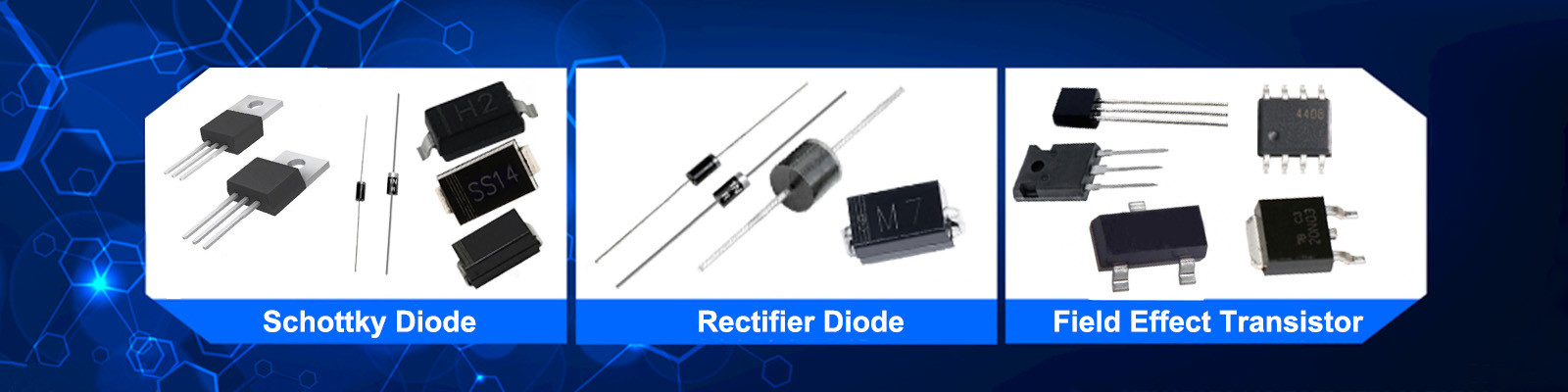
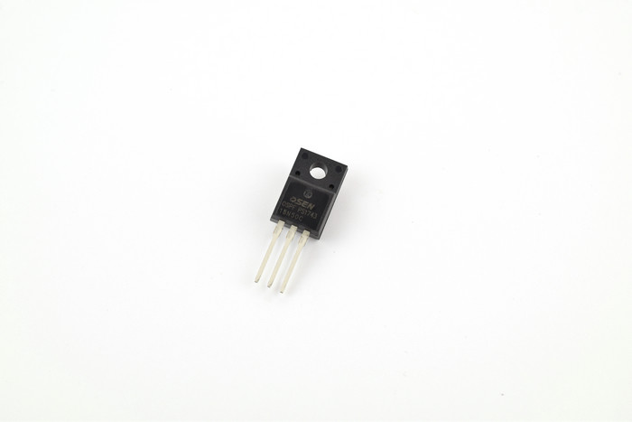
Original Mosfet Power Transistor / Plastic P Channel Transistor
Mosfet Power Transistor Features
Low gate charge
Low Rdson(typical 5.5mΩ)
Fast switching
100% avalanche tested
Improved dv/dt capability
RoHS product
Mosfet Power Transistor Applications
Absolute Maximum Ratings (Tc=25°C)
| Symbol | Parameters | Ratings | Unit |
| VDSS |
Drain-Source Voltage |
500 | V |
| VGS |
Gate-Source Voltage-Continuous |
±30 | V |
| ID |
Drain Current-Continuous(Note 2) |
18 | A |
| IDM |
Drain Current-Single Plused(Note 1) |
56 | A |
| PD |
Power Dissipation (Note 2) |
52 | W |
| Tj |
Max.Operating junction temperature |
150 | ℃ |
Electrical characteristics (Tc=25°C unless otherwise noted)
| Symbol | Parameters | Min | Typ | Max | Units | Conditions | |
| Static Characteristics | |||||||
| BVDSS |
Drain-Source Breakdown |
500 | -- | -- | V | ID=250µA,VGS=0V,TJ=25°C | |
| VGS(th) |
Gate Threshold Voltage |
3.0 | -- | 5.0 | V | VDS=VGS,ID=250μA | |
| RDS(on) |
Drain-Source On-Resistance |
-- | 0.4 | 0.7 | Ω | VGS=10V,ID=6.5A | |
| IGSS |
Gate-Body Leakage Current |
-- | -- | ±100 | nA | VGS=±30V,VDS=0 | |
| IDSS |
Zero Gate Voltage Drain Current |
-- | -- | 1 | μA | VDS=500V,VGS=0 | |
| Switching Characteristics | |||||||
| Td(on) |
Turn-On Delay Time |
-- | 25 | 60 | ns |
VDS=250V,ID=13A, |
|
| Tr |
Rise Time |
-- | 100 | 210 | ns | ||
| Td(off) |
Turn-Off Delay Time |
-- | 130 | 270 | ns | ||
| Tf |
Fall Time |
-- |
100 |
210 | ns | ||
| Qg |
Total Gate Charge |
-- | 43 | 56 | nC |
VDS=400,VGS=10V, |
|
| Qgs |
Gate-Source Charge |
-- | 7.5 | -- | nC | ||
| Qgd |
Gate-Drain Charge |
-- | 18.5 | -- | nC | ||
| Dynamic Characteristics | |||||||
| Ciss |
Input Capacitance |
-- | 1580 | 2055 | pF |
VDS=25V,VGS=0, |
|
| Coss |
Output Capacitance |
-- | 180 | 235 | pF | ||
| Crss |
Reverse Transfer Capacitance |
-- | 20 | 25 | pF | ||
| IS |
Continuous Drain-Source Diode |
-- | -- | 13 | A | ||
| VSD |
Diode Forward On-Voltage |
-- | -- | 1.4 | V | IS=13A,VGS=0 | |
| Rth(j-c) |
Thermal Resistance, Junction to |
-- | -- | 2.58 | ℃/W | ||
Our Advantage:
1. Electronic component specialist and professional.
2. Strong R & D team, experienced research staffs
3. Strong and consistent quality control, same standard as of RoHS.
4. Elite sales team with more than 5 years international trading experience individually.
5. Strong technical support to help customers choose the most appropriate products.
6. Be proud of the product and the competitive price.
![]()
![]()
![]()
![]()

