
| Place of Origin: | Jiangxi, China |
|---|---|
| Brand Name: | JC |
| Certification: | RoHS |
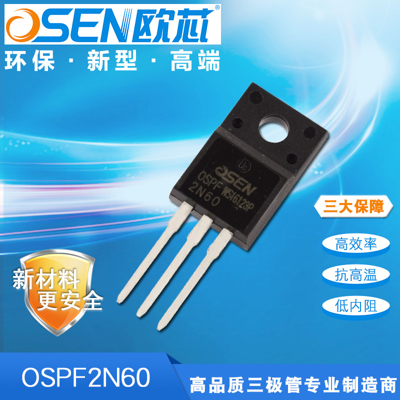
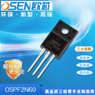
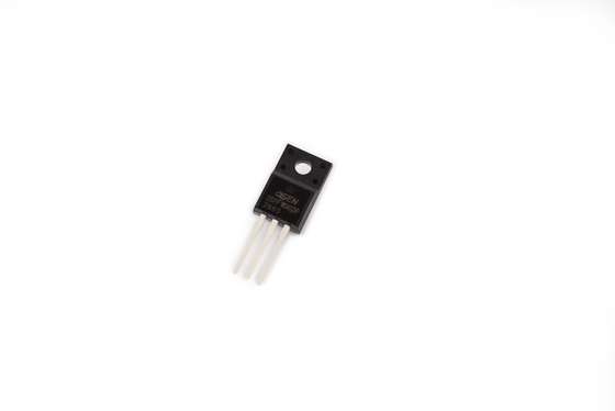
| Model Number: | OSPF2N60 |
| Minimum Order Quantity: | Negotiable |
| Price: | Negotiated |
| Packaging Details: | Boxed |
| Delivery Time: | 1 - 2 Weeks |
| Payment Terms: | Telegraphic Transfer in Advance (Advance TT, T/T) |
| Supply Ability: | 15,000,000PCS Per Day |
| Name: | N Channel Transistor | Drain-Source Voltage: | 600V |
|---|---|---|---|
| Gate-Source Voltage-Continuous: | ±30V | Drain Current-Continuous(Note 2): | 2A |
| Drain Current-Single Plused(Note 1): | 8A | Power Dissipation (Note 2): | 23W |
| High Light: | mosfet power transistor,high power transistor |
||
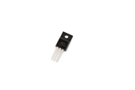
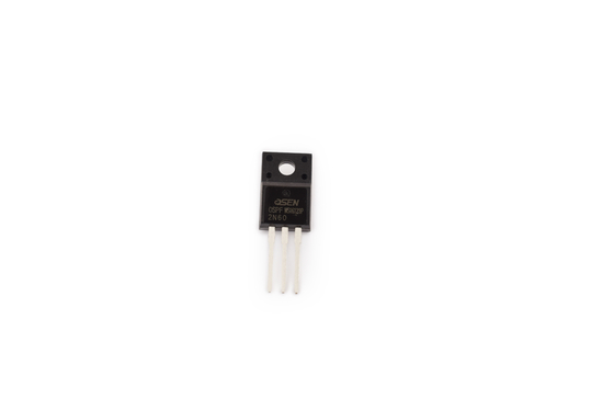
High Input Impedance N Channel Transistor , Field Emission Transistor 600V
N Channel Transistor Features
N Channel Transistor Applications
Absolute Maximum Ratings (Tc=25°C)
| Symbol | Parameters | Ratings | Unit |
| VDSS |
Drain-Source Voltage |
600 | V |
| VGS |
Gate-Source Voltage-Continuous |
±30 | V |
| ID |
Drain Current-Continuous(Note 2) |
2 | A |
| IDM |
Drain Current-Single Plused(Note 1) |
8 | A |
| PD |
Power Dissipation (Note 2) |
23 | W |
| Tj |
Max.Operating junction temperature |
150 | ℃ |
Electrical characteristics (Tc=25°C unless otherwise noted)
| Symbol | Parameters | Min | Typ | Max | Units | Conditions | ||
| Static Characteristics | ||||||||
| BVDSS |
Drain-Source Breakdown VoltageCurrent (Note 1) |
600 | -- | -- | V | ID=250µA,VGS=0V,TJ=25°C | ||
| VGS(th) |
Gate Threshold Voltage |
2.0 | -- | 4.0 | V | VDS=VGS,ID=250μA | ||
| RDS(on) |
Drain-Source On-Resistance |
-- | 3.6 | 4.0 | Ω | VGS=10V,ID=1A | ||
| IGSS |
Gate-Body Leakage Current |
-- | -- | ±100 | nA | VGS=±30V,VDS=0 | ||
| IDSS |
Zero Gate Voltage Drain Current |
-- | -- | 1 | μA | VDS=600V,VGS=0 | ||
| gfs |
Forward Transconductance |
1.0 | -- | -- | S | VDS=15V,ID=1A | ||
| Switching Characteristics | ||||||||
| Td(on) |
Turn-On Delay Time |
-- | 40 | 60 | ns |
VDS=300V,ID=2A, RG=25Ω(Note 2) |
||
| Tr |
Rise Time |
-- | 35 | 55 | ns | |||
| Td(off) |
Turn-Off Delay Time |
-- | 70 | 95 | ns | |||
| Tf |
Fall Time |
-- | 45 | 65 | ns | |||
| Qg |
Total Gate Charge |
-- | 9 | 15 | nC |
VDS=480V,VGS=10V, ID=2A(Note 2)
|
||
| Qgs |
Gate-Source Charge |
-- | 1.5 | -- | nC | |||
| Qgd |
Gate-Drain Charge |
-- | 4.5 | -- | nC | |||
| Dynamic Characteristics | ||||||||
| Ciss |
Input Capacitance |
-- | 260 | 350 | pF |
VDS=25V,VGS=0, f=1MHz
|
||
| Coss |
Output Capacitance |
-- | 38 | 50 | pF | |||
| Crss |
Reverse Transfer Capacitance |
-- | 8 | 20 | pF | |||
| IS |
Continuous Drain-Source Diode Forward Current(Note 2) |
-- | -- | 2 | A | |||
| VSD |
Diode Forward On-Voltage |
-- | -- | 1.4 | V | IS=2A,VGS=0 | ||
| Rth(j-c) |
Thermal Resistance, Junction to Case |
-- | -- | 5.5 | ℃/W | |||
Our Service
1. Efficient Servicer: Professional and Efficient services, Feedback in 24 hours. Full range products for choice.
2. Factory Choice: We are professional supplier. OEM / ODM are Available. We also supply search service for you if you need . We have professional purchasing department to supply the latest goods and best seller products.
3. QC Service: Great Quality Check, We know how to do good check quality. We have 19 years experience professional QC team.
4. Logistic Service: We would like to assist our customer to make QC + collect goods from other supplier.
5. Long-Term Service: We are looking for long-term business PARTNER! So we supply excellent service and can design as your request.
![]()
![]()
![]()
![]()

