

| Place of Origin: | Jiangxi, China |
|---|---|
| Brand Name: | JC |
| Certification: | RoHS |
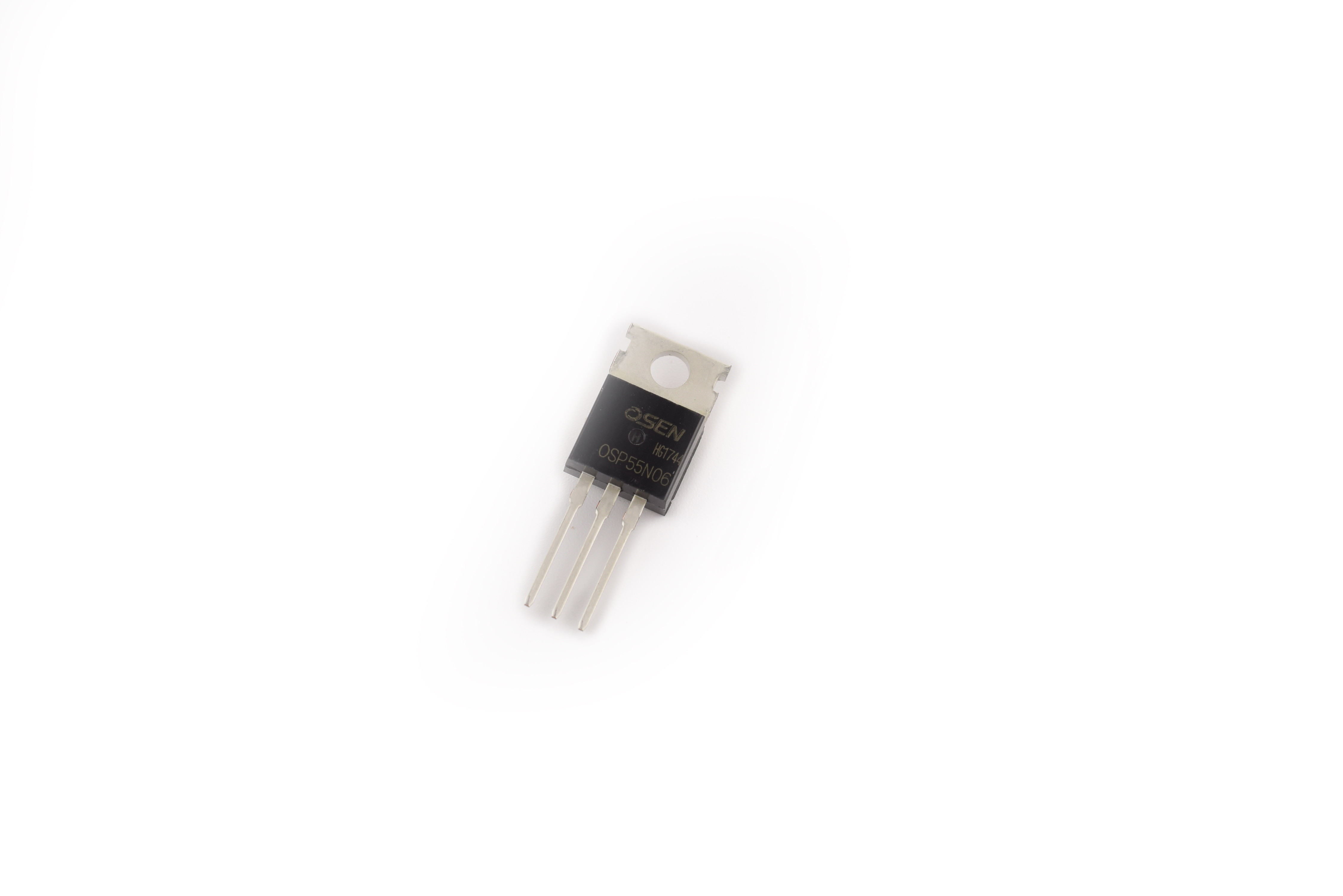
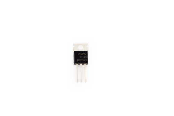
| Model Number: | OSP55N06- |
| Minimum Order Quantity: | Negotiable |
| Price: | Negotiated |
| Packaging Details: | Boxed |
| Delivery Time: | 1 - 2 Weeks |
| Payment Terms: | Telegraphic Transfer in Advance (Advance TT, T/T) |
| Supply Ability: | 15,000,000PCS Per Day |
| Name: | N Channel Field Effect Transistor | Drain-Source Voltage: | 60V |
|---|---|---|---|
| Gate-Source Voltage-Continuous: | ±20V | Drain Current-Continuous(Note 2): | 55A |
| Drain Current-Single Plused(Note 1): | 200A | Power Dissipation (Note 2): | 130W |
| High Light: | mosfet power transistor,high power transistor |
||
Organic N Channel Field Effect Transistor For Electronic Lamp Ballast
N Channel Field Effect Transistor Features
Absolute Maximum Ratings (Tc=25°C)
| Symbol | Parameters | Ratings | Unit |
| VDSS | Drain-Source Voltage | 60 | V |
| VGS | Gate-Source Voltage-Continuous | ±20 | V |
| ID | Drain Current-Continuous(Note 2) | 55 | A |
| IDM | Drain Current-Single Plused(Note 1) | 200 | A |
| PD | Power Dissipation (Note 2) | 130 | W |
| Tj | Max.Operating junction temperature | 150 | ℃ |
Electrical characteristics (Tc=25°C unless otherwise noted)
| Symbol | Parameters | Min | Typ | Max | Units | Conditions | ||
| Static Characteristics | ||||||||
| BVDSS | Drain-Source Breakdown | 60 | -- | -- | V | ID=250µA,VGS=0V,TJ=25°C | ||
| VGS(th) | Gate Threshold Voltage | 2.0 | -- | 4.0 | V | VDS=VGS,ID=250μA | ||
| RDS(on) | Drain-Source On-Resistance | -- | 18 | 22 | mΩ | VGS=10V,ID=25A | ||
| IGSS | Gate-Body Leakage Current | -- | -- | ±100 | nA | VGS=±20V,VDS=0 | ||
| IDSS | Zero Gate Voltage Drain Current | -- | -- | 1 | μA | VDS=60V,VGS=0 | ||
| gfs | Forward Transconductance | 15 | -- | -- | S | VDS=30V,ID=25A | ||
| Switching Characteristics | ||||||||
| Td(on) | Turn-On Delay Time | -- | 60 | -- | ns | VDS=30V,ID=25A, | ||
| Tr | Rise Time | -- | 185 | -- | ns | |||
| Td(off) | Turn-Off Delay Time | -- | 75 | -- | ns | |||
| Tf | Fall Time | -- | 60 | -- | ns | |||
| Qg | Total Gate Charge | -- | 39 | -- | nC | VDS=48V,VGS=10V, | ||
| Qgs | Gate-Source Charge | -- | 9.3 | -- | nC | |||
| Qgd | Gate-Drain Charge | -- | 13 | -- | nC | |||
| Dynamic Characteristics | ||||||||
| Ciss | Input Capacitance | -- | 880 | -- | pF | VDS=25V,VGS=0, | ||
| Coss | Output Capacitance | -- | 430 | -- | pF | |||
| Crss | Reverse Transfer Capacitance | -- | 110 | -- | pF | |||
| IS | Continuous Drain-Source Diode | -- | -- | 55 | A | |||
| VSD | Diode Forward On-Voltage | -- | -- | 1.4 | V | IS=20A,VGS=0 | ||
| Rth(j-c) | Thermal Resistance, Junction to Case | -- | -- | 1.15 | ℃/W | |||
Our Company
Shenzhen Canyi Electronics Technology Co., Ltd. was established in 2000. After more than ten years of development, it has become a professional agent of well-known electronic component brands at home and abroad.
![]()
![]()
![]()
![]()

